Service hotline 0755-83261303
Email:ht@htsemi.com
Address315 Huachang Road, Dalang Street, Longhua District, Shenzhen

How to choose a suitable BGA package?
According to the power consumption and heat dissipation requirements of the chip, the BGA package with good heat dissipation performance is selected. Chips with high power consumption usually require better cooling solutions. For example, when choosing a
30
2024-07

What are the advantages of BGA packaging? What is the difference between other packaging methods?
Traditional pin packages (such as DIP, SOP, etc.) usually arrange the pins of the chip on either side or around the package. The BGA package distributes the pins of the chip throughout the bottom and connects them with spherical solder joints. This layout
24
2024-07

What is BGA packaging? What are the basics of BGA packaging?
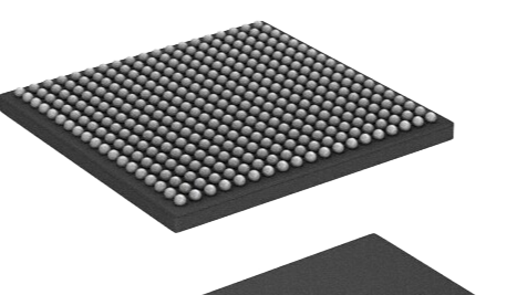
This Package can accommodate more pins than other packages such as Dual in-line packages or Quad Flat packages, and the entire bottom surface of the device can be used as pins instead of only around it. It also has a shorter average wire length than the s
23
2024-07

An article on understanding the model rules and parameter meanings of field-effect transistors
There are currently two naming methods for field-effect transistors. The first naming method is to use the third letter J of the model to represent the junction field-effect transistor and O to represent the insulated gate field-effect transistor. The sec
23
2024-04

The working principle, characteristics, and function of field-effect transistors
Field Effect Transistor (FET) stands for Field Effect Transistor. A typical transistor is called a bipolar transistor due to the participation of two types of polar carriers, namely the majority carrier and the reverse polarity minority carrier, in conduc
22
2024-04
Recruitment
0755-83240725
Cooperation
QQ:3001784606
3001784606

Tel
0755-83261303
Message